|
Shenzhen Hengda Electronics Limited
|
Gold Index: 11458
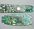
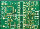
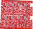
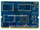
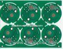
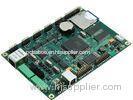
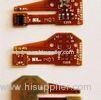
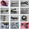
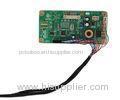
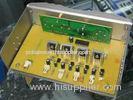
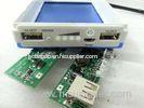
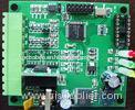
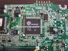
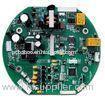
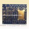
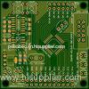
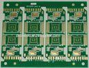
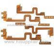
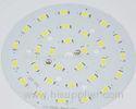
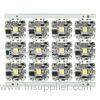
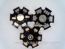
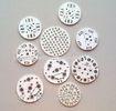
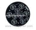
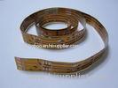
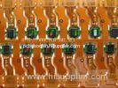
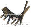
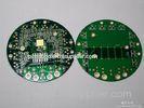
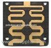
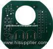
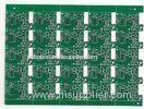
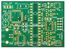
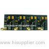
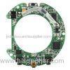
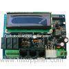
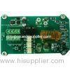
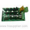
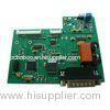
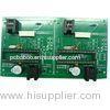
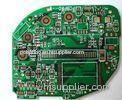
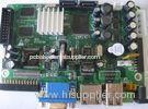
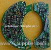
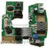
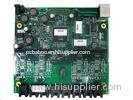
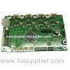
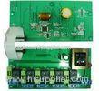
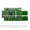
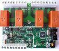
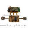
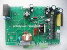
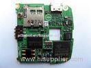
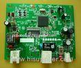
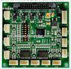
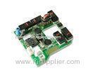
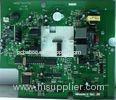
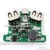
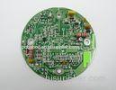
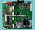
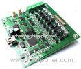
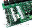
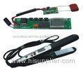
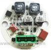
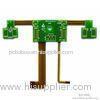
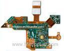
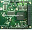
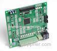
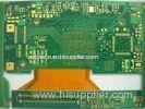
Touch Screen Rigid-Flex Printed Circuit Boards Stiffener Polyimide 1 OZ Copper FPC
| Place of Origin: | Zhejiang, China (Mainland) |
|
|
|
| Add to My Favorites | |
| HiSupplier Escrow |
Product Detail
Touch Screen Rigid-Flex Printed Circuit Boards Stiffener Polyimide 1 OZ Copper FPC Quick Det
Touch Screen Rigid-Flex Printed Circuit Boards Stiffener Polyimide 1 OZ Copper FPC
Quick Details
PCB Type: | Flexible Printed Circuit |
Layer : | 2 layer |
Min .Line Width/Space: | 3mil/3mil |
Min. Via Diameter: | 0.3mm |
Finish Thickness: | 1.2mm |
Surface Finish: | ENIG |
Size: | 60*100MM |
Material: | PI |
Color: | Gold |
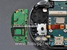
Application: | Touch Screen |
Description
Shenzhen Hengda Electronics is a leading manufacturer of precision Flexible Printed Circuit (FPC) for customers worldwide. We specialize in quick-turn FPC prototypes to FPC mass productions, provide high quality and cost effective turn key solutions to our customers.

This table lists the standard flex circuits materials and material thicknesses that we may have daily available. If the material or thickness you require is not listed, consult us. We have full specification of each material available for your required.
FPC Materials
Material Function | Material Type | Options |
Flexible Insulator | Polyimide(PI) | 1/2 mil to 5 mil |
Conductor | Copper | 1/4 oz(0.009mm) to 10 oz(0.356mm) |
Rigid Substrate (Rigid-Flex) | FR-4 | 3 mil to 125 mil |
Adhesive | Acrylic Adhesive | 1/2 mil to 3 mil |
Adhesiveless Material also available | ||
Stiffener | FR-4 Polyimide(PI) Polyester(PET) Adhesivetape Steel/Aluminum/Copper | 3mil to 125 mil 1/2 mil to 5mil 1 mil to 15mil 6 mil |
Solder Mask | Polyimide(PI) PhotoimageableCoverlay Liquid Photoimageable Covercoat | 1/2 mil to 5 mil 1 mil to 2.5 mil Liquid Typically for surface mount and dense applications |
Surface Finish Options | Tin | Immersion Tin |
Gold | Electrolytic Nickel Immersion Gold Electrolytic Hard Nickel /Gold Electrolytic Soft Nickel/Gold | |
Silver | Immersion Silver | |
OSP | OSP | |
Shielding | Solid Copper Crosshatched Copper Conductive Silver Aluminum | Required To Limited Electromagnetic and/or Electrostatic |
FPC Standard Structure

Technical Capabilities
Layer (Max) | Up to 8 Layers | |
Board Size (Max) | 500*1000mm | |
Outer tolerance | a+/-0.2mm Hand Trim | |
Hole | Diameter(Min) | 0.1mm(Finished) |
| Diameter Tolerance | a.Plating Through Holes+/-0.08mm b.Non-Plating Through Holes+/-0.05mm |
| Drill Position Tolerance | +/-0.076mm |
Conductor | Width Tolerance | +/-15% |
Spacing(Min) | 2mil | |
Spacing Tolerance | +/-15% | |
Pad | Pad(Non-Wiring) | >=0.04mm+ Hole |
Pad(Wiring) | >=0.3mm+Hole | |
Coverlay | Coverlay to Pad(Min) | 100um |
Coverlay to Conductor (Min) | 100um | |
Coverlay Width(Min) | 250um | |
Stiffener holes | >=0.25mm+Access hole | |
FPC Application

Testing Procedures
We perform multiple quality assurance procedures before shipping out any PCB board. These include:
- Visual Inspection
- Flying probe
- Bed of nails
- Impedance control
- Solder-ability detection
- Digital metallograghic microscope
- AOI (Automated Optical Inspection)
Quick turn lead times
For HDI PCB production, we can provid 7 to10 days turn around times. For multilayer PCBs, the fastestturnaround time depends on the number of layers and quantity.
Service Guarantee
We make sure to serve each customer professionally, truthfully and friendly to the best of our ability. We will gladly re-work your project if your project isn’t 100% satisfactory.
Get a quick quote now
By sending in a bill of material, ge
Related Search
Find more related products in following catalogs on Hisupplier.com
Company Info
Shenzhen Hengda Electronics Limited [China (Mainland)]
Business Type:Manufacturer
City: Shenzhen
Province/State: Guangdong
Country/Region: China (Mainland)


