|
Shenzhen Hengda Electronics Limited
|
Gold Index: 11458


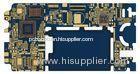
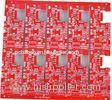
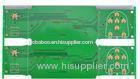
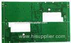
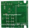
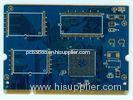
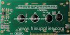
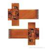
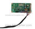
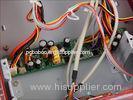
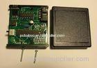
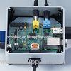
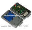
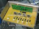
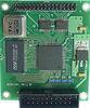
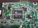
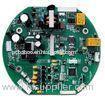
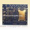
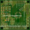
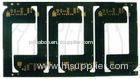
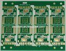
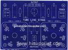
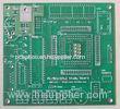
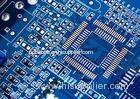
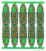
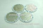
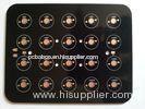
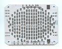
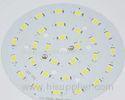
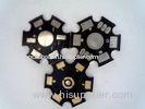
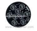
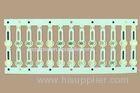
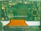
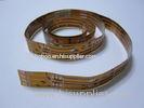
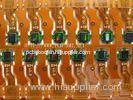
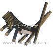
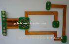
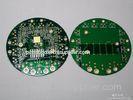
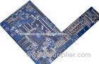
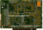
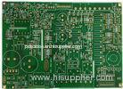
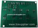
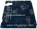
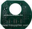
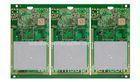
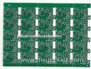
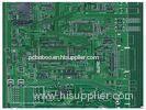
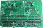
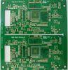
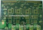
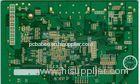
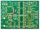
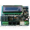
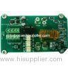
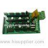
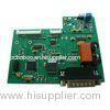
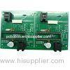
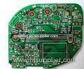
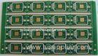
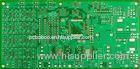
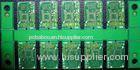
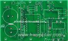
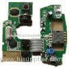
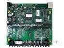
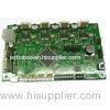
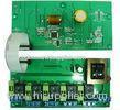
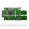
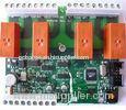
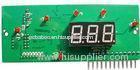
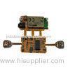
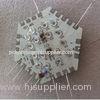
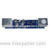
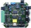
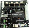
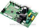
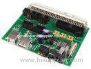
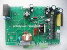
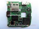
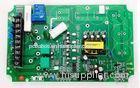
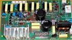
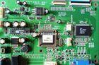
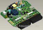
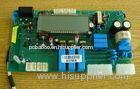
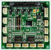
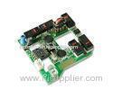
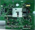
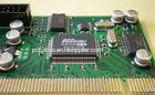
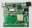
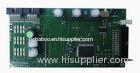
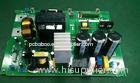
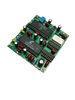
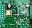
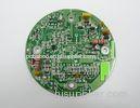
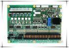
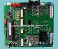
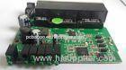
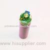
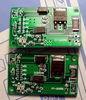
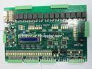
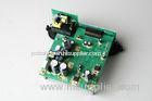
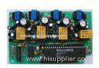
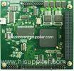
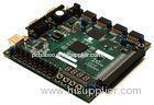
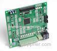
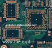
Production HDI PCB Design 3 Level Gold Finger Finish With Laser Pits
| Place of Origin: | Zhejiang, China (Mainland) |
|
|
|
| Add to My Favorites | |
| HiSupplier Escrow |
Product Detail
Production HDI PCB Design 3 Level Gold Finger Finish With Laser Pits
<str
Production HDI PCB Design 3 Level Gold Finger Finish With Laser Pits
Quick Details
|
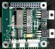
PCB Type: |
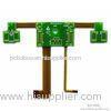
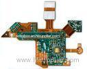
HDI PCB |
|
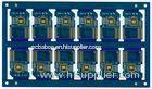
Layer : |
8 layer |
|
Min .Line Width/Space: |
3mil/3mil |
|
Min. Via Diameter: |
0.3mm |
|
Finish Thickness: |
1.6mm |
|
Surface Finish: |
Gold Finger |
|
Size: |
120*150MM |
|
Material: |
FR-4 |
|
Color: |
Green |
|
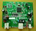
Application: |
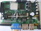
Computer |
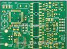
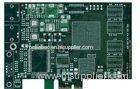
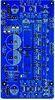
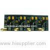
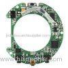
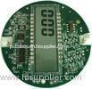
Description
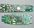
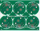
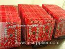
We have a professional HDI (high density interconnect) circuit board manufacturing base; we attach importance to HDI technology R&D to satisfy customer's HDI technology requirements.
The HDI PCBs we offer include the following highly requested characteristics:
- Blind and/or buried vias
- Via-in-pad
- Through vias from surface to surface
- 20 um circuit geometries
- 30 um dielectric layers
- 50 um laser vias
- 125 um bump pitch processing
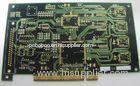
Our high density circuit boards have the technology pushing capabilities to drive applications in a large number of industries including but not limited to semiconductor test equipment, defense, medical and aerospace.

Below is our latest Any layer HDI technology:

Technical Capabilities
|
Number of layers |
1, 2, 4 or 6, up to 36 layers |
|
Order Quantity |
1 to 500,000 |
|
Board shape |
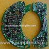
Rectangular, round, slots, cutouts, complex, irregular |
|
Board type |
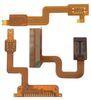
Rigid, flexible, rigid-flexible |
|
Board material |
FR4 glass epoxy, FR4 High Tg, RoHS compliant; Aluminum, Rogers, etc. |
|
Board cutting |
Shear, V-score, tab-routed |
|
Board thickness |
Flex, 0.2 ~ 6.0 mm, 0.01 ~ 0.25″ |
|
Copper weight |
1.0, 1.5, 2.0 Oz |
|
Solder mask |
Double-sided green LPI, Also support red, white, yellow, blue, black |
|
Silk screen |
Double-sided or single-sided in white, yellow, black, or negative |
|
Silk screen min line width |
0.006″ or 0.15mm |
|
Max board dimensions |
45 x 45″ or 114 x 114 cm |
|
Min trace/gap |
0.004”, 0.1mm, or 4 mils |
|
Min drill hole diameter |
0.006”, 0.15mm, or 6 mils |
|
Surface finish |
HASL,Nickle, Imm Gold,Imm Tin,Imm Silver, OSP etc. |
|
Board thickness tolerance |
±10% |
|
Copper weight tolerance |
±0.25 oz |
|
Minimal slot width |
0.12”, 3.0 mm, or 120 mils |
|
V-score depth |
20-25% of board thickness |
|
Plated through holes |
Yes |
|
Sink holes |
Yes |
|
Design file format |
Gerber RS-274X, 274D, Eagle and AutoCAD’s DXF, DWG |
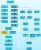
PCB Production Flow Chart

Testing Procedures
We perform multiple quality assurance procedures before shipping out any PCB board. These include:
- Visual Inspection
- Flying probe
- Bed of nails
- Impedance control
- Solder-ability detection
- Digital metallograghic microscope
- AOI (Automated Optical Inspection)
Quick turn lead times
For HDI PCB production, we can provid 7 to10 days turn around times. For multilayer PCBs, the fastestturnaround time depends on the number of layers and quantity.
Service Guarantee
We make sure to serve each customer professionally, truthfully and friendly to the best of our ability. We will gladly re-work your project if your project isn’t 100% satisfactory.
Get a quick quote now
By sending in a bill of material, gerber files including assembly drawing and we will have a quotation back to you within hours. With Shenzhen hengda there is never a hidden cost and our prices are very competitive and reasonable.
Related Search
Find more related products in following catalogs on Hisupplier.com
Company Info
Shenzhen Hengda Electronics Limited [China (Mainland)]
Business Type:Manufacturer
City: Shenzhen
Province/State: Guangdong
Country/Region: China (Mainland)